Re-Architecting the AI Data Center Network with Co-Packaged Optics
For years, data center networking followed a familiar formula. Switch ASICs handled packet forwarding, pluggable optical modules sat at the front panel, and fiber carried data across racks and rows. Each layer improved independently. Silicon got faster, optics delivered more bandwidth, and fiber remained a reliable transport medium. The separation was clean with compute on the inside, optics at the edge, and fiber in between.
But that split is now breaking down, and that’s not because optics stopped working. In the new era of data center networking for AI training, everything around the optics has changed.
AI clusters, especially at hyperscale, have pushed bandwidth, power, and density requirements into a scenario where the weakest link has become the few centimeters of copper between the switch chip and the front panel. In other words, the problem is no longer transmitting data across the entire data center. Instead, the problem is efficiently getting data from the ASIC to the optics in the first place.
That is the problem co-packaged optics (CPO) is trying to solve.
The Real Bottleneck
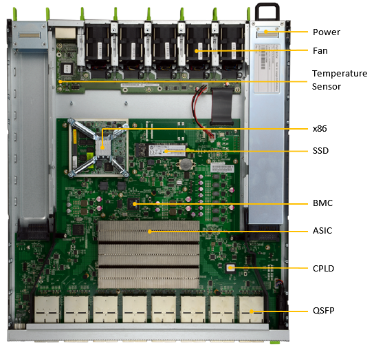
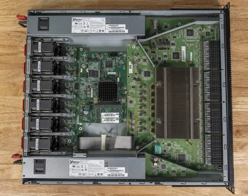
Inside a traditional Ethernet switch, the switch ASIC sits near the center of the board. That means there needs to be a physical communication pathway between the middle of the board and the optics on the front panel. To do this, ASICs communicate (externally) using high-speed SerDes lanes printed right into the board. In the image below on the left you can see the ASIC located just off of the center. In the image on the right, you can see the heatsink covering the Tomahawk 1 ASIC.
A SerDes (Serializer/Deserializer) converts wide parallel data inside the chip into extremely high-speed serial streams specifically for physical transmission. Modern switch ASICs operate at incredible speeds with today’s leading designs using 112G PAM4 signaling and the industry quickly moving toward 224G PAM4.
PAM4 (Pulse Amplitude Modulation with four signal levels) encodes two bits per symbol instead of one, effectively doubling bandwidth compared to traditional binary signaling. But it also dramatically reduces signal margin, making transmission far more sensitive to noise and distortion which creates a major problem.
Specifiically, at these data rates, even very short distances (the ASIC to the optic) introduce significant attenuation, reflections, and distortion in the signal. The channel can exceed 30 dB of loss depending on layout complexity, forcing designers to treat the PCB itself as a carefully engineered transmission medium rather than simple wiring.
To compensate, modern systems rely heavily on signal conditioning. For example, equalization techniques such as continuous-time linear equalization and decision feedback equalization are used to compensate for channel loss. Also, full DSPs (digital signal processors) inside the optical module are often required to retime and reconstruct the signal before optical conversion.
These techniques work, but the cost is high. They consume a lot of power, generate additional heat, and introduce latency through multiple layers of signal recovery and conditioning. And as data rates continue scaling toward 800G and 1.6T systems, the margin for error shrinks so dramatically that the electrical channel itself becomes the limiting factor.
What Changes with Co-Packaged Optics
Co-packaged optics fundamentally changes the electrical-to-optical boundary inside the switch.
At a high level, co-packaged optics rethinks where optical conversion happens inside a network switch. Instead of treating optics as removable front-panel components, CPO integrates optical components directly alongside the switch silicon. The result isn’t just faster networking, but a broader architectural shift toward tighter integration between compute, switching, and communication.
In other words, instead of putting optical modules at the edge of the switch chassis, Co-Packaged Optics moves the optics much closer to the switch ASIC by placing them in literally the same physical package or directly beside it.
And even though the reduction in distance may only be a few centimeters, the impact is massive. In the image below on the left, you can see the evolution starting at the top and going down from pluggable optics to CPO. In the image below on the right, notice how the optics engine is, in this case, immediately adjacent to the ASIC on the same substrate. The substrate is one of two foundational layers for the ASIC itself. It’s usually the base silicon wafer on which the switching transistors are built, or it could be the underlying material that physically connects the silicon die itself to the main circuit board.
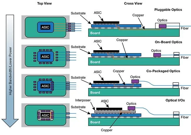
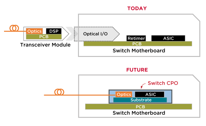
Source: Broadcom. Illustration of traditional switch I/O vs. CPO integrated design
Rather than sending high-speed electrical signals across (relatively) long printed circuit board traces to the front panel, the ASIC now routes those signals over extremely short electrical channels, often through silicon interposers, organic substrates, or advanced redistribution layers, directly into nearby photonic engines.
These photonic engines might use silicon photonics, indium phosphide lasers, or hybrid integrated optical assemblies, depending on the vendor design. But regardless of implementation, the key is that the electrical channel is no longer the primary scaling bottleneck.
Also, because the channel loss is dramatically reduced, the equalization requirements mentioned above can be simplified. In a CPO design, SerDes architectures can operate with lower voltage swings and less analog front-end complexity. That also means that in many designs, DSP-heavy retiming stages traditionally embedded inside pluggable modules can be simplified, reduced, or located somewhere else in the system.
The result is a measurable reduction in energy consumed per transmitted bit, which is one of the most important metrics in modern AI infrastructure.
Collapsing the Electrical Channel
One of the most important concepts in CPO is what many engineers describe as “collapsing the electrical channel.”
Traditional pluggable systems have to tolerate worst-case channel conditions involving PCB routing loss, connector discontinuities, package escape challenges, and module variability. As signaling moves toward 224G PAM4, the available eye opening becomes so small that maintaining signal integrity across those channels becomes extremely difficult.
With co-packaged optics, the channel between the ASIC and optical engine can shrink to sub-centimeter distances inside tightly controlled impedance environments. Lower-loss channels allow reduced equalization overhead, simplified SerDes architectures, and lower transmit voltage requirements. Collectively, this reduces power consumption across the electrical side of the link. And today power matters more than ever.
AI clusters already push data center power budgets to extreme levels. Networking infrastructure alone can consume megawatts at hyperscale deployments. Even modest reductions in picojoules-per-bit become enormously valuable when multiplied across hundreds of thousands of optical lanes.
This means that at its core, co-packaged optics is as much a power-efficiency technology as it is a bandwidth technology.
Thermal Engineering Changes Completely
Beyond bandwidth and power efficiency, CPO introduces an entirely new set of thermal engineering challenges. As optical engines move closer to the switch silicon, the thermal profile of the entire system changes.
In pluggable architectures, optical modules are decoupled from the switch ASIC and dissipate heat at the front panel, often in airflow regions that are already restricted by the chassis design. This leads to localized hotspots that need careful thermal zoning within the chassis.
In CPO architectures, optical engines are co-located with the ASIC, which changes the thermal coupling problem. The switch ASIC is still the dominant heat source, but now optical components must be engineered to tolerate higher and more dynamic thermal environments.
This drives tighter integration of thermal design at the package level, including advanced heat spreaders, microfluidic or vapor chamber cooling designs in some experimental systems, and careful wavelength stabilization strategies for temperature-sensitive laser components.
At the same time, system-level airflow design can improve because the front panel is no longer densely packed with high-power optical modules. This can simplify chassis-level thermal engineering even if package-level complexity increases. So in other words, CPO doesn’t eliminate thermal complexity - it relocates it.
Bandwidth Density and Radix Scaling
Another major driver behind co-packaged optics is bandwidth density.
Modern high-end switch ASICs are already targeting 51.2T and 102.4T class bandwidths, with internal SerDes counts scaling into the hundreds or even thousands of high-speed lanes. Mapping this bandwidth onto traditional front-panel pluggables becomes very impractical due to the actual mechanical spacing on the board, power delivery, and thermal dissipation limitations. CPO changes this equation entirely.
Because optical I/O can be distributed across the package substrate rather than concentrated at the faceplate, bandwidth density scales far more efficiently. Switch designers are no longer constrained by the physical geometry of front-panel optics.
This is especially important in AI fabrics, where extremely high radix (port count) switching is critical for minimizing oversubscription and improving collective communication performance.
Latency Means Marginal Gains but System-Level Impact
At the individual link level, the latency reduction from CPO can seem relatively small, often measured in nanoseconds rather than microseconds. However, hyperscale AI systems operate very differently from traditional enterprise networks.
Large-scale AI training depends heavily on collective communication operations like all-reduce and all-to-all exchanges, where thousands of GPUs continuously synchronize data throughout the training process. In these environments, even small reductions in network overhead can compound significantly across the cluster.
CPO helps reduce some of that overhead by shortening the electrical path and minimizing the DSP-heavy retiming stages commonly found in pluggable optics. Fewer signal recovery stages can reduce serialization delays and simplify portions of the data path.
Individually, these gains might seem incremental, but at hyperscale, they are not.
When synchronization occurs constantly across thousands of GPUs, small latency reductions accumulate into measurable improvements in overall training efficiency and job completion time. This means CPO is not purely a latency optimization technology. Instead, it’s part of a broader architectural shift toward minimizing every possible source of network overhead.
The Manufacturing Problem
Despite the advantages of co-packaged optics, the transition from traditional pluggables to CPO leads to a new challenge in manufacturing.
Traditional pluggable optics benefit from decades of ecosystem maturity, standardized form factors, and multi-vendor interoperability. CPO breaks much of that modularity. Now ASIC vendors, photonics vendors, packaging companies, and foundries have to tightly coordinate design and manufacturing processes in a way they haven’t before.
Optical components now have to be aligned with extremely high precision, which makes manufacturing more difficult. Testing, repairs, and replacement also become more complicated because the optics are built directly into the system instead of being removable modules.
Silicon photonics has become one of the dominant enabling technologies in this space due to its compatibility with CMOS processes, but most systems still need external laser sources or hybrid integration approaches.
Long story short: the engineering challenge is huge, and that’s why the industry is investing in its solution.
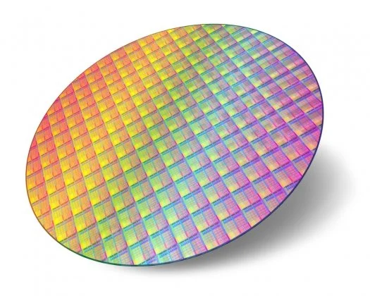
A 300mm silicon wafer, typical of the size used in network switches
Coexistence, Not Replacement
Despite the architectural advantages of co-packaged optics, the industry isn’t moving toward immediate replacement of pluggables. Instead, the current trajectory is one of coexistence driven by workload segmentation.
Pluggables still make sense in environments where modularity, serviceability, and interoperability matter more than absolute efficiency. Enterprise networks and moderate-bandwidth environments still benefit from flexible front-panel optics.
CPO, on the other hand, is being targeted at high-radix, high-bandwidth AI switching layers where power efficiency, bandwidth density, and thermal optimization dominate design constraints. This creates a growing split in optical networking architecture with traditional modular optics at the edge and aggregation layers, and tightly integrated optical-electrical co-design inside the AI fabric core.
The Bigger Picture
Co-packaged optics should be viewed as an intermediate step in a broader transition toward optical-centric system design. As electrical interconnect scaling gets closer to physical limits, and as AI workloads continue demanding more bandwidth, the industry will likely move toward even tighter integration designs. This means optical I/O directly on compute packages, and eventually, chip-to-chip optical fabrics within rack-scale systems.
In that sense, CPO represents a shift in abstraction from treating optics as detachable peripherals to treating them as an integral part of the switching system itself.
The implications extend beyond networking hardware. They redefine how system architects think about the boundary between compute and communication. And in the AI era, that boundary is becoming less distinct with every generation.
Similar Articles